
Different excitations, including electronic, photonic, and polaritonic ones, are associated with characteristic length scales over which their interaction with the environment becomes significant. Structuring matter at these scales can provide access to confinement-induced quantization, modified dispersion, and collective dynamics that are otherwise difficult to realize. The three examples below (electrons in 2D materials, phonon polaritons in boron nitride, and spin waves in solid-state ensembles) illustrate several instances in which this general principle can be brought to bear on sensing and integrated source platforms.
Bandstructure Engineering in 2D Materials — A Platform for Nanometer-Scale Quantum Confinement
For electrons in two-dimensional materials, the relevant length scale is the de Broglie wavelength, typically in the 1–100 nm range. As feature sizes approach this regime, quantum confinement effects can become significant. Periodic or quasi-periodic potential landscapes at these scales restrict the electronic modes supported by the material and can therefore be used to influence band structure, transport, and coupling. Several routes have been explored toward this objective, including etching, applied strain, patterned gating, and twisted layer stacks, although each comes with tradeoffs in resolution, tunability, or scalability. As a result, much of this regime remains experimentally challenging to access in a controlled and scalable fashion.
In [1], we explore one route toward this regime by repurposing atomic layer deposition (ALD), a thin-film deposition technique with atomic-scale thickness control, as a surface-structuring method. By depositing thin oxide layers across widely spaced nanofins, we form nanolaminate surfaces with in-plane feature sizes down to 1.75 nm over wafer-scale areas. When graphene is placed across these patterned surfaces and used as a gate-defined platform, we observe satellite Dirac peaks consistent with confinement-induced modifications of the electronic structure. More broadly, the sub-10 nm regime is also relevant to a range of other phenomena, including excitonic confinement in transition-metal dichalcogenides, substrate-mediated moiré engineering, valley control, deep-UV nanophotonics, and quantum recoil in free-electron–light interactions. In that sense, this fabrication platform may provide a useful experimental handle across several areas of nanoscale physics.
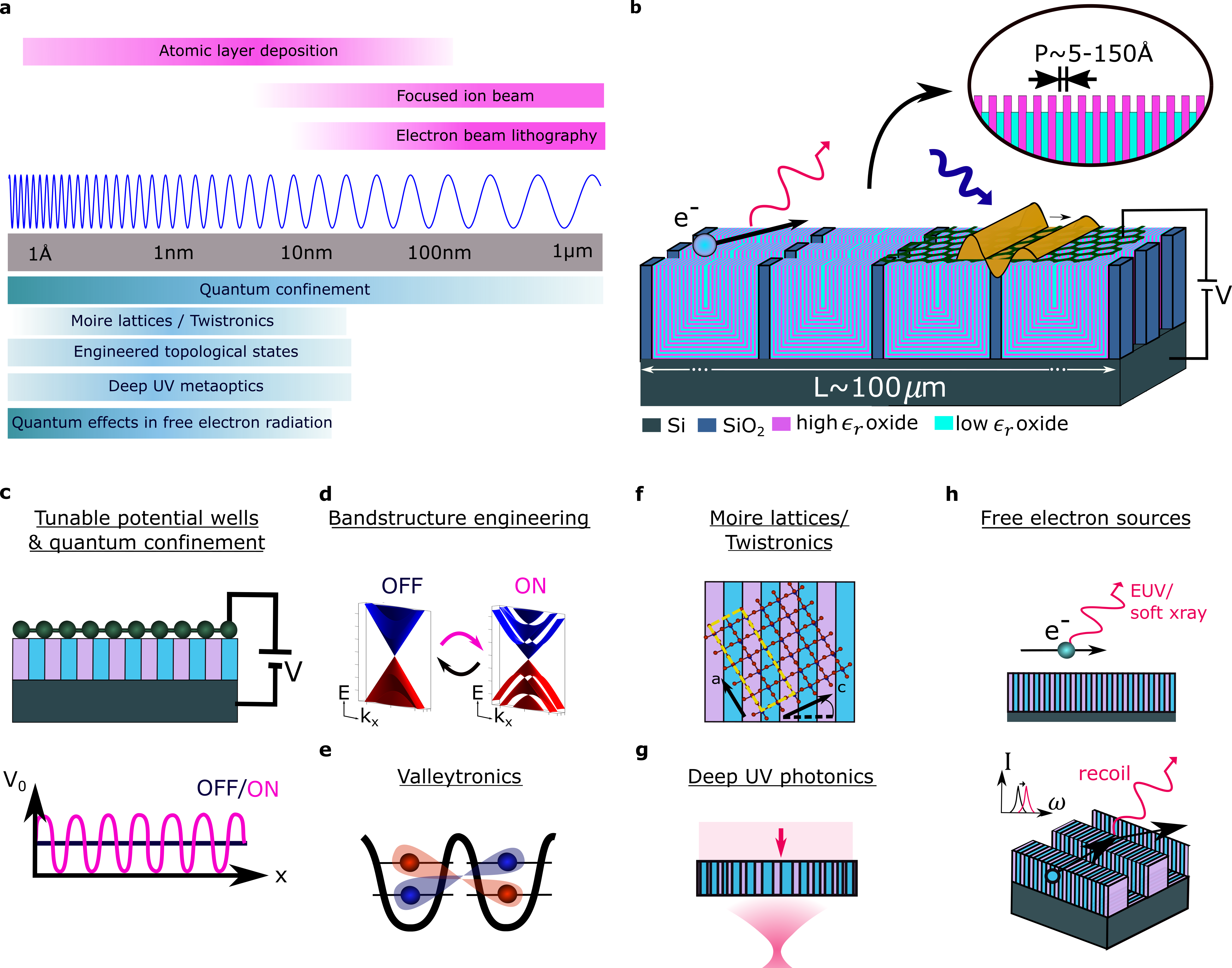
Nanolaminate platform to attain extreme regimes of light-matter interactions [1]. (a) Comparison of feature sizes accessible to various nanofabrication techniques (pink) against physical phenomena that become significant at corresponding length scales (blue). (b) Schematic of the proposed platform, relying on widely spaced oxide pillars to transform sub-nm thick layers grown by ALD into a nanolaminated surface. (c–h) Applications in extreme light–matter interactions: tunable superlattices, band-structure engineering, quantum dot formation, substrate-controlled moiré superlattices, deep-UV photonic control, and free-electron radiation sources accessing soft x-ray regimes.
Reconfigurable Polaritonic Devices via van der Waals Heterostructures
Phonon polaritons in van der Waals materials such as hexagonal boron nitride (hBN) exhibit strong subwavelength confinement, making them promising for compact integrated photonic devices. Combining such polaritonic media with phase-change materials (PCMs) offers a route toward reconfigurable control of polariton propagation at the nanoscale, potentially enabling tunable refractive and meta-optical functionalities without relying solely on static lithographic patterning. Because of the strong field confinement of these modes, such platforms are of interest for applications including surface-sensitive spectroscopy, biosensing, and photodetection. More generally, the reconfigurability of PCM-based heterostructures suggests a possible route toward programmable polaritonic devices.
In [2], we demonstrate this idea in an hBN-GST heterostructure. By locally switching the GST refractive index using optical writing, we pattern the substrate on subwavelength scales and thereby control the propagation of phonon polaritons in the overlying hBN. This allows the implementation of rewritable two-dimensional refractive and meta-optical elements, including a metasurface lens that focuses the polariton mode to near its diffraction limit. Because these patterns can be erased and rewritten, the platform provides a flexible way to study and implement programmable polaritonic circuits.
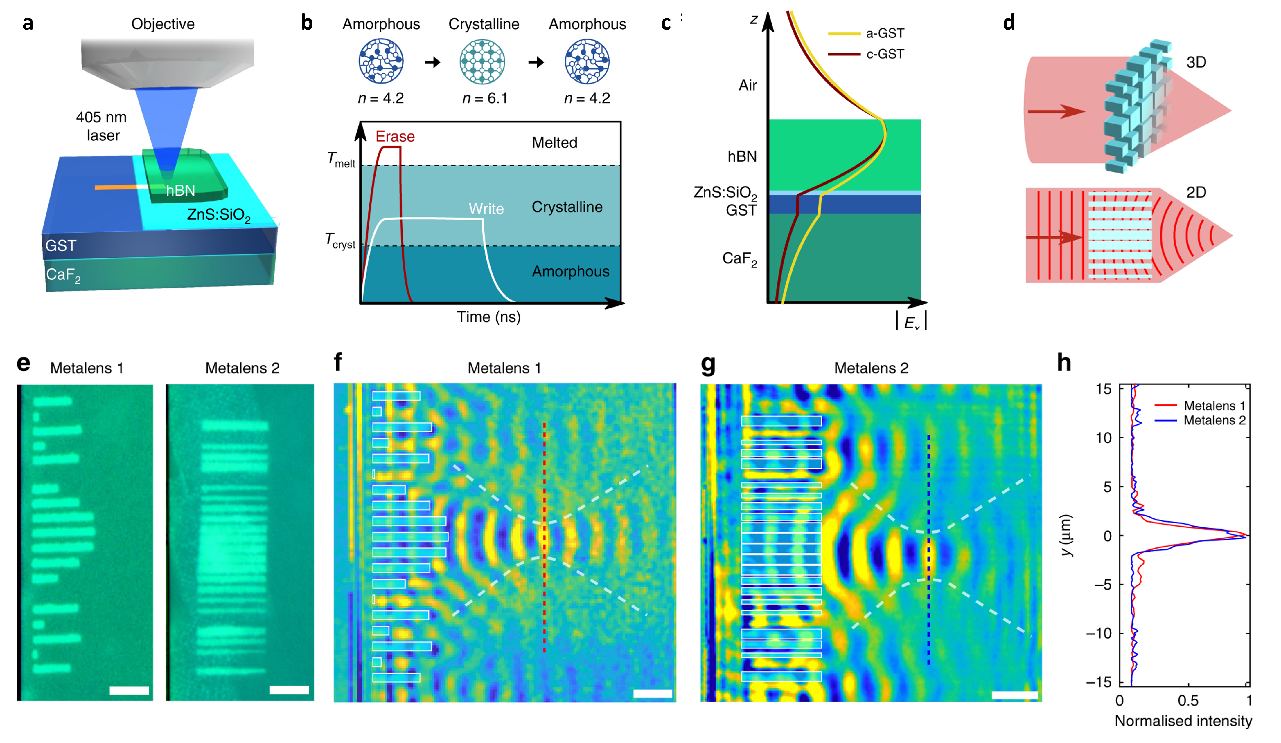
Rewritable metaoptics for phonon polaritons [2]: The dispersion of phonon polaritons in hexagonal boron nitride (hBN) can be controlled through patterning of the surrounding material. (a–c) Phase change materials (PCMs) have two material phases of drastically different refractive indices, switchable optically and electrically, allowing reconfigurable control of polariton propagation. (d–h) Example of a 2D metasurface focusing the phonon polariton mode to its diffraction limit; the structure was erased and rewritten between metasurfaces 1 and 2.
Controlling Many-Body Interactions of Solid-State Quantum Emitters
Solid-state quantum emitters — including quantum dots and spin defects such as nitrogen-vacancy (NV) centers in diamond — are likewise highly sensitive to their local environment. In dense ensembles, where emitters interact strongly through dipolar coupling, this opens a route to collective quantum dynamics that can amplify weak signals and ultimately surpass classical sensing limits. However, imperfections and positional disorder pose major obstacles to coherent correlated behavior.
In [3], we demonstrate that this barrier can be overcome by combining time-dependent nanoscale magnetic field gradients with Hamiltonian engineering. By imprinting and probing nanometer-scale spin spirals across the ensemble, we observe a disorder-resilient collective spin evolution, establishing a pathway toward interaction-enhanced quantum metrology and nanoscale imaging of materials and biological systems under ambient conditions.
Related publications: * denotes equal contribution
[1] Spaegele, C.M. et al. A scalable platform for nanometer-scale quantum confinement. (in review) [2] Chaudhary, K.*, Tamagnone, M.*, Yin, X.*, Spaegele, C.M.*, Oscurato, S.L., Li, J., Persch, C., Li, R., Rubin, N.A., Jauregui, L.A. and Watanabe, K., 2019. Polariton nanophotonics using phase-change materials. Nature Communications, 10(1), p.4487. [3] Put, P.*, Leitao, N.T.*, Gao, H.*, Spaegele, C.M.*, Makarova, O., Hughes Wyatt, L.B., Maccabe, A.C., Mammen, M., Machielse, B., Zhou, H., Pustelny, S., Bleszynski Jayich, A.C., Capasso, F., Martin, L.S., Park, H. and Lukin, M.D. Collective many-body dynamics in a solid-state quantum sensor controlled through nanoscale magnetic gradients. arXiv:2506.11920 (2025). [4] Tamagnone, M., Chaudhary, K., Spaegele, C.M., Zhu, A., Meretska, M., Li, J., Edgar, J.H., Ambrosio, A. and Capasso, F., 2019. High quality factor polariton resonators using van der Waals materials. arXiv preprint arXiv:1905.02177.